(China (Mainland))


Product Summary
-
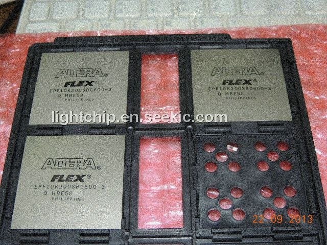
The EPF10K200SBC600-3 is an embedded Programmable Logic Device. Based on reconfigurable CMOS SRAM elements, the FLEX architecture incorporates all features necessary to implement common gate array megafunctions. With up to 200,000 typical gates, the EPF10K200SBC600-3 provides the density, speed, and features to integrate entire systems, including multiple 32-bit buses, into a single device.
Parametrics
EPF10K200SBC600-3 absolute maximum ratings: (1)VCCINT, Supply voltage With respect to ground: –0.5 to 3.6 V; (2)VCCIO: –0.5 to 4.6 V; (3)VI, DC input voltage: –2.0 to 5.75 V; (4)IOUT, DC output current, per pin: –25 to 25 mA; (5)TSTG, Storage temperature No bias: –65 to 150℃; (6)TAMB, Ambient temperature Under bias: –65 to 135℃; (7)TJ, Junction temperature: 135℃.
Features
EPF10K200SBC600-3 features: (1)Embedded programmable logic devices (PLDs), providing system-on-a-programmable-chip (SOPC) integration in a single device: Enhanced embedded array for implementing megafunctions such as efficient memory and specialized logic functions; Dual-port capability with up to 16-bit width per embedded array block (EAB); Logic array for general logic functions; (2)High density: 30,000 to 200,000 typical gates (see Tables 1 and 2); Up to 98,304 RAM bits (4,096 bits per EAB), all of which can be used without reducing logic capacity; (3)MultiVoltTM I/O pins can drive or be driven by 2.5-V, 3.3-V, or 5.0-V devices; (4)Low power consumption; (5)Bidirectional I/O performance (tSU and tCO) up to 212 MHz; (6)Fully compliant with the PCI Special Interest Group (PCI SIG) PCI Local Bus Specification, Revision 2.2 for 3.3-V operation at 33 MHz or 66 MHz; (7)-1 speed grade devices are compliant with PCI Local Bus Specification, Revision 2.2, for 5.0-V operation; (8)Built-in Joint Test Action Group (JTAG) boundary-scan test (BST) circuitry compliant with IEEE Std. 1149.1-1990, available without consuming additional device logic.
Diagrams
EPF10K200SBC600-3