Product Summary
-
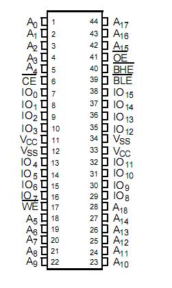
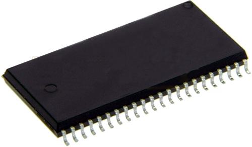
The cy7c1051dv33-10zsxi is a high-performance CMOS Static RAM organized as 512K words by 16 bits. Write to the cy7c1051dv33-10zsxi by taking Chip Enable (CE) and Write ) Enables (WE) inputs LOW. Read from the device by taking Chip Enable (CE) and Output Enable (OE) LOW while forcing the Write Enable (WE) HIGH. If Byte HIGH Enable (BHE) of the cy7c1051dv33-10zsxi is LOW, then data from memory will appear on IO8 to IO15. The cy7c1051dv33-10zsxi is available in a 44-pin TSOP II package with center power and ground (revolutionary) pinout, as well as a 48-ball fine-pitch ball grid array (FBGA) package.
Parametrics
cy7c1051dv33-10zsxi absolute maximum ratings: (1) Storage Temperature: -65 to +150°C; (2) Ambient Temperature with Power Applied: -55 to +125°C; (3) Supply Voltage on VCC to Relative GND: -0.5 to +4.6V; (4) DC Voltage Applied to Outputs in High-Z State: -0.3 to VCC +0.3V; (5) DC Input Voltage: -0.3 to VCC +0.3V; (6) Current into Outputs (LOW) : 20mA; (7) Static Discharge Voltage: >2001V (per MIL-STD-883, Method 3015) ; (8) Latch-up Current: >200 mA.
Features
cy7c1051dv33-10zsxi features: (1) High speed tAA=10ns; (2) Low active power: ICC=110mA@10ns; (3) Low CMOS standby power ISB2=20mA; (4) 2.0V data retention; (5) Automatic power-down when deselected; (6) TTL-compatible inputs and outputs; (7) and OE features Easy memory expansion with CE; (8) Available in lead-free 48-ball FBGA and 44-pin TSOP II packages.
Diagrams

| Image | Part No | Mfg | Description |  |
Pricing (USD) |
Quantity | ||||||||||||
|---|---|---|---|---|---|---|---|---|---|---|---|---|---|---|---|---|---|---|
 |
 CY7C1051DV33-10ZSXI |
 Cypress Semiconductor |
 SRAM 8M FAST ASYNC IND HI SPD SRAM |
 Data Sheet |

|
|
||||||||||||
 |
 CY7C1051DV33-10ZSXIT |
 Cypress Semiconductor |
 SRAM 8M FAST ASYNC HI SPD SRAM |
 Data Sheet |

|
|
||||||||||||
 (China (Mainland))


